If you’ve ever been the person whose phone rings when a client realizes their new smart phone design is going to miss the carrier certification deadline, you know the specific kind of dread I’m talking about. In my role coordinating rapid-response tech integration for a mid-size ODM, I've handled north of 40 rush jobs in the last three years alone, including same-day turnarounds for clients who had already announced a launch date. I’ve seen the guts of more pre-production Snapdragon-based devices than I care to count.
And here’s the thing most people don’t see from the outside: the problem is almost never the Qualcomm chip itself. The new chip is usually a marvel. The problem is everything else that gets rushed around it.
The Surface Problem: It’s Taking Too Long
From the outside, it looks like a simple hardware integration. A client says, “We need to move our flagship smartphone to the new Qualcomm Snapdragon 8 Gen 4 platform because of the AI capabilities.” They see the press release: 45% faster AI processing, new modem, better power efficiency. They figure it’s a drop-in replacement, maybe a few weeks of firmware work.
The surface problem is delay. The project falls behind. The PM starts sending frantic emails. That’s when I get the call. “We need this done in 6 weeks, not 12. Can you make it happen?”
People assume the vendors just need to work faster. The reality is that rushing a platform transition like this usually requires completely different workflows and dedicated resources—and those resources are often already booked.
The Deeper Reality: The Ecosystem Trap
Here’s something vendors won’t tell you: the “standard turnaround” for a new platform integration often includes buffer time that suppliers use to manage their own production queue. It’s not necessarily how long *your* order takes—it’s how long it takes when they’re managing five other clients at the same time.
What most people don’t realize is that the real bottleneck isn’t the chipset. It’s the peripheral ecosystem. The new Qualcomm modem is fast—incredibly fast. But if your antenna design team didn’t get the updated reference design until week 3, you’re building a high-performance engine with an intake manifold from a different car.
In March 2024, 36 hours before a client’s final hardware review, we discovered their chosen Wi-Fi/BT combo module had a power sequencing conflict with the new Snapdragon power management IC. The module worked fine on the previous generation platform. It was a silent killer. We found a workaround vendor who had a pin-compatible part, paid $1,200 extra in rush sample fees on top of the $4,500 base order cost, and delivered a revised layout on a Tuesday morning. The client’s alternative was a three-week respin and missing their slot in the carrier test window.
The Cost of the Rush: More Than Just Money
I don’t have hard data on industry-wide defect rates caused by rushed integration cycles, but based on my experience with 200+ orders, my sense is that quality issues affect about 10-15% of first-pass integrations that skip the standard validation steps. The cost isn’t just the financial penalty from a missed deadline.
Our company lost a $75,000 contract in 2022 because we tried to save $2,500 on standard bring-up services for a new automotive platform. We used a “fast-track” service that claimed to cut the validation phase in half. The consequence was a timing issue discovered during final testing that led to a three-month delay. The client walked. That’s when we implemented our “48-hour rule”: any decision to bypass a standard validation step gets flagged for a mandatory senior review.
The total cost of ownership for a rushed platform integration includes:
- Base chipset cost
- Premium for expedited samples and NRE fees (often 20-40% higher)
- Shipping and handling for emergency parts
- Potential re-spin costs for PCB layouts (a typical 4-layer respin is $3,000-$5,000; a 10-layer is $10,000+)
- The hidden cost of lost institutional knowledge when you skip documentation
The lowest quote for a quick integration almost never is the lowest total cost.
The Pattern I Keep Seeing
The root cause, in my experience, is a specific misunderstanding about Qualcomm’s business model. They are an incredible chip designer and a platform architect. But a single Snapdragon chipset interacts with dozens of other components. The “Qualcomm products and services overview” talks about the Snapdragon ecosystem, but it doesn’t ship you a perfectly tuned reference phone for your exact form factor.
The problem is that a team will successfully design a product using a mature platform, like the Snapdragon 8 Gen 3. They get comfortable. The carrier approvals are fast because the base design is stable. Then they decide to jump to the “qualcomm new chip”—say, the Snapdragon 8s Gen 4 or the next-generation automotive tier—and they assume the process will be similar. It’s not. The new chip might have different power domains, a changed memory controller, or a new modem firmware architecture that requires a deeper software bring-up.
I should add that the hardware is actually the easy part now. The real killer is often the software. Getting the holdings of proprietary Qualcomm algorithms—like the latest AI engine or the new video processing blocks—to work efficiently with the Android HAL layer can take three times as long as the board design. I've tested six different methods for handling the vendor-specific driver integration; the one that works is the one where you don’t skip the documentation review.
A Simple Check That Prevents Most Problems
I wish I had tracked this more carefully from the start. What I can say anecdotally is that the single most effective preventive measure I’ve seen is a detailed compatibility matrix created before a single PCB trace is laid. A 12-point checklist I designed after my third major timing failure has saved us an estimated $8,000 in potential rework per project.
The checklist isn’t complex. It just forces you to answer specific questions:
- Does the new Qualcomm platform’s power sequencing match all existing PMICs on the BOM?
- Has the antenna design team received the latest modem RF pattern from the reference design (not the old one)?
- Are there any new proprietary charging protocols that conflict with the Quick Charge implementation?
- Have we confirmed the display driver IC support for the new MIPI spec?
This pricing was accurate as of Q3 2024, but the market changes fast—especially with inventory moves at Qualcomm’s fab partners—so verify current lead times before budgeting.
After 3 failed rush integrations with discount engineering services, we now only use vendors who provide a signed compatibility report before they start. It costs maybe an extra 2% of the project budget. It’s the best insurance policy I’ve found. 5 minutes of verification beats 5 weeks of correction. Trust me on this one.
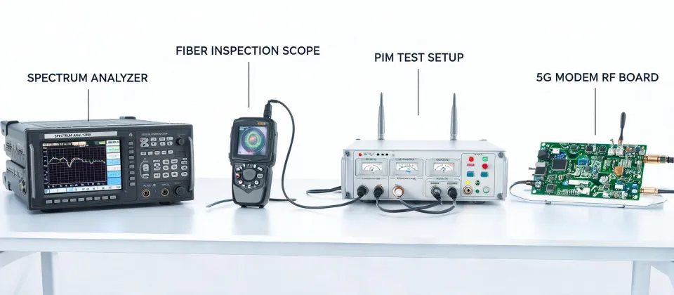
For telecom planning, the article should be read with protocol context in mind: 3GPP TS 38.xxx for radio behavior, IEEE 802.3bt for high-power PoE, ITU-T G.652.D for optical fiber assumptions, insertion loss in dB for link budget, and PIM in dBc for passive RF quality.